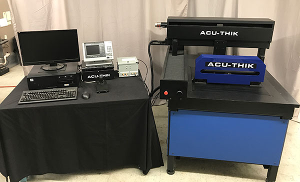
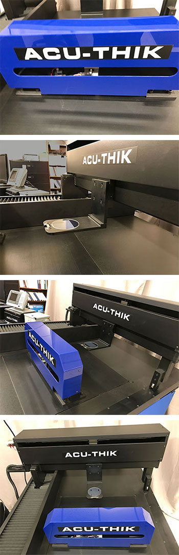
 ACU-THIK™ is an automated thickness measurement tool incorporating dual contact probes for high accuracy inspection of semiconductor wafers. ACU-THIK™ can be configured to accommodate wafer diameters of 100mm – 400mm and beyond. ACU-THIK™’s patent pending design can help diagnose and control the following:
• Thickness: The distance through a wafer between corresponding X/Y points on a front and back surface. Thickness is calculated to resolution and repeatability of .00025mm/.00001” (ten millionths of an inch).
• Bow: The deviation of the center point of the median surface of a free, unclamped wafer from the median surface reference plane established by three or more points at equidistant locations on the wafer.
• Warp: The differences between the maximum and minimum distances of the median surface of a free, unclamped wafer from a reference plane. By examining the entire wafer and by virtue of incorporating more comprehensive data points, warp is a more useful measurement of true wafer shape.
• Validation of System, Pre and Post Measurement: ACU-THIK™ calculates the thickness of a certified gage block, prior to the inspection of the wafer and after the conclusion of the wafer inspection routine. This validation ensures the integrity of the data collection for each wafer inspection.
The X/Y location for each thickness data point will be automatically output to MS Excel for further analysis. Programming software runs on Windows 10 and comes complete as a turnkey system. ACU-THIK™ can obtain X/Y/Thickness data points at a rate of 15 points/minute, allowing for greater throughput and more accurate thickness/flatness definition of wafers.